Engineering with 'The very
atoms, all the way down!'
| Research lines |
| Highlighted Publications |
| Teaching |
| Outreach |
| CV |
| home |
News |
||
|
||
|
DAVID SERRATE DONOSO | ||||||||||||||||||
Engineering with 'The very atoms, all the way down!'
|
|||||||||||||||||||
|
A) Ultrathin stacks of polar insulators. I suggest the use of a Scanning Tunneling Microscope (STM) tip as writing and reading head of bistable ground state on a ferroelectric surface. This surface consists of stacks of ultrathin insulating layers that exhibit an artificially induced spontaneous electric polarization, which can be reversed with the STM tip. The ultimate spatial resolution of STM for probing and building this kind of ferroelectric materials, brings the study of ferroelectricity and its fundamental properties down to the atomic scale. |
|
|||||||||||||||||
| B) Magnetism at the atomic scale. Spin-polarized STM provides single spin sensitivity, which in combination with lateral atomic manipulation; allow us to assemble artificial nanostructures with designated exchange coupling and function. Quantum spin properties and their applications in quantum information processing are investigated by inelastic tunnelling spectrosopy with energy resolution of 0.1 meV. | |||||||||||||||||||
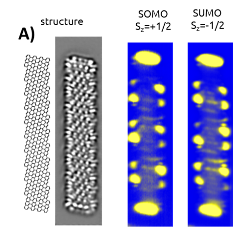
| C) On-surface synthesis of covalent molecular nanostructures (CMNs). The potential of organic chemistry is combined with the high spatial and energy resolution of SPM to produce graphene like structures with a palette of electronic, optical and magnetic properties. The surface facilitates the reactions by catalytical activation of intermediates and 2D confinement of reactants. This leads to defect free 2D molecular crystals whose properties can be tailored by choosing the geometry and functional groups of the monomer building blocks. This processes occur typically on metals, but it would be desirable to transfer the CMNs to other more technologically relevant surfaces. In order to avoid the transfer, we study synthesis strategies directly on functional surfaces such as those studied in tasks A and B. | |||||||||||||||||||